

The World Leaders in Plasma Diagnostic Instruments #PlasmaMeasurement #IntelligentSensors #MeasuringTheImpossible #ThinFilms #Semiconductors #PlasmaDiagnostics
Ireland
Joined June 2009
- Tweets880
- Following973
- Followers532
- Likes463
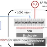





Plasma enhanced chemical vapor deposition uses plasma of ionized species to deposit high quality thin films. PECVD process uses both energy from plasma and thermal energy on substrate to achieve desired chemical reaction for thin film growth.
buff.ly/3Hji0Pi

Follow @Impedans for more industry updates.
ALE can be achieved using sequential, self-limiting thermal reactions. ALE and ALD can enable the fabrication of many advanced three-dimensional semiconductor structures. Read more.
buff.ly/3vHF1be

Thin film deposition techniques apply thin material coatings in-order to modify the surface properties of engineering components. There are two types of thin film deposition techniques chemical vapor deposition and physical vapor deposition.
buff.ly/3xp6Vqk

Follow @Impedans for more industry updates.
The semiconductor market is expected to return to a semblance of balance throughout the rest of the year, as analyst firm Gartner forecasts 13.6 per cent growth to US$676 billion for the end of 2022.
buff.ly/36QNuiK

Follow Impedans for more industry updates.
Nearly all semiconductor manufacturing processes utilize chemical vapor deposition. Three commonly used CVD techniques can be found in modern manufacturing of devices such as CMOS and MEMS ICs, RF Switches, etc.
buff.ly/2Tm3imS

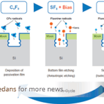
Creating high aspect ratio microstructures is one of the key processes in the advanced MEMS field. The Bosch process is capable of producing deep features with exceptional anisotropy, etch-rate, and etch mask selectivity.
buff.ly/2Y36575

Reactive ion etching is a technique in which masked material is subjected to a shower of ions in the presence of reactive gases in-order to enhance the material removal process. Read more.
buff.ly/3xI0Usx

Sputtering is a PVD process used for depositing materials onto a substrate There are a number of ways to enhance this process. One common way to do this is to use what is known as a magnetron sputtering system. Read more.
buff.ly/3jXXUjs

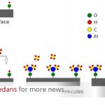
Atomic layer deposition is a vapor phase technique used to coat surfaces with thin films. The film is deposited layer by layer so that the chemical composition and coating thickness can exactly be defined. Read more to know how the classical ALD works.
buff.ly/3xB9yci

Follow @Impedans
In the manufacturing of semiconductor devices, etching corresponds to any technique that removes material systematically from a thin layer on a platform and leaves behind a sequence of that substance on the platform. Read more.
buff.ly/3kaaAEl

Follow @Impedans
Atomic Layer Deposition (ALD) uses one or more volatile precursors or gases to deposit high quality thin films on desired substrates with precision controlled at angstrom length scale. Read more to understand the step in ALD cycle.
buff.ly/3M9pd6M

If enough energy is added to a gas, the gas molecules become ionized, carrying a net positive charge, this state is called plasma. Plasma technology is commonly used in many industries, including in the automotive, microelectronics, etc.
buff.ly/3gve6GR

Plasma etching is the removal of material from surfaces via plasma processes. Read more to know about different plasma etching techniques.
buff.ly/3uFkUtG

How the fundamental science of plasma surface interaction can contribute to atomic-scale accuracy with little or no damage to the materials in device fabrication? Read more.
buff.ly/37btQyc

The process for depositing and creating thin film coating over a substrate material is known as thin film deposition. These coating also have various characteristics that are leveraged for improving or altering some element of the substrate performance.
buff.ly/3jsLwIa

Follow Impedans for industry updates.
RF sputtering is a thin film coating technique. RF Sputtering runs an energetic wave through an inert gas in a vacuum chamber which becomes ionized. Read more to know about various advantages of RF sputtering.
buff.ly/36XsBT2

Plasma Enhanced Atomic Layer Deposition (PEALD) is a thin film deposition technique used for producing high quality epitaxial thin film. PEALD use chemical precursors in which each precursors are carefully selected and introduced in specific order.
buff.ly/3u5kFb5

The deposition of thin films on a surface is used for modification of the physical or chemical properties of the surface of the coated material. They can change its optical, electrical and thermal properties.
buff.ly/35wc2Nv

Etching is a process carried out after the #photolithography step, which involves removing of unwanted materials from a #wafer. #Silicon wafer manufacturers use two main types of #etching: wet etching and dry etching. Read more
buff.ly/3tSGM4D

Semiconductor manufacturing requires a high level of purity and cleanliness within the manufacturing environment. Using robots to handle microscopic parts has become essential in introducing micro and nanotechnology for semiconductor manufacturers.
buff.ly/3K9pkyF
