

I develop AI inference Chips/SoCs for a living. Read my work and subscribe to my newsletter at https://xitter.cf/t.co/RGu9NKu1Ze
Santa Clara, CA
Joined June 2009
- Tweets140
- Following52
- Followers1.2K
- Likes181



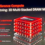



$ALAB PCIe-based scale-up solution looks promising on performance and latency.
But how does the cost compare to Ethernet-based scale-up? PCIe cables and the required retimers aren’t cheap.
I asked Astera about this, and they said a TCO white paper is coming next week. Curious to see the numbers.


Hot take: Jensen’s pick to succeed him at NVIDIA might just be Ian Buck.
Deeply technical. Invented CUDA. Helped turn NVIDIA into the AI powerhouse it is today.
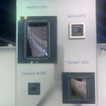
A pic of him holding NVIDIA’s CPO switch chip at OCP Global Summit happening right now.


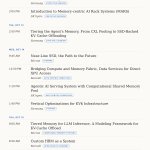
I'll be at OCP this week. Here are the sessions I'm attending in Memory/Storage, Networking, and Systems.
The ones I won't miss:
Mon 5:45pm · Ian Buck, NVIDIA keynote
Tue 11:10am · Partha Ranganathan, Google keynote
Tue 2:50pm · Samsung on CXL pooling and SSD-backed KV cache offload
Thu 8:20am · Marvell on custom HBM, co-designing the base die, D2D power, and package thermals
Full schedule in the images.


Subbu retweeted

To clients I've spoken to, I maintain that 3D DRAM integration in HBC is a technically sound approach.
- It expands capacity while maintaining SRAM like performance
- The pj/bit consumed while moving bits makes it a good approach for power constrained edge devices
In this quick episode, @austinsemis sits down with Durga Malladi from QCOM for a quick chat on @semidoped to find out more.
Check it out.

🎙️ NEW EPISODE: Qualcomm's HBC vs HBM, Dragonfly AI 250, and Winning on TCO
Austin sits down with Qualcomm's Durga Malladi live in Maui to talk HBC (High Bandwidth Compute). HBC is Qualcomm's differentiated bet to win data center inference workloads.
HBM shuttles data across wide buses to a separate accelerator. HBC puts compute directly on the stacked DRAM's logic die.
- HBM is fast but power-hungry; HBC drops latency AND power per bit
- 18x effective bandwidth on the AI 250 at the SAME 768 GB and SAME 160 kW
- A trillion-parameter FP4 model on a single card
- Foundry + memory-vendor relationships de-risk multi-megawatt supply at scale
Chapters:
0:00 Introduction
2:49 The Memory Wall Problem
8:05 HBC Physical Architecture
9:33 HBC vs. Custom HBM
11:50 Silicon Proof Points Coming
12:08 Managing Thermals
13:34 Dragonfly AI 250
14:48 Trillion-Parameter Model on One Card
16:56 Tokenomics and TCO
18:26 Why TCO is Key
19:26 Manufacturing at Scale
Get more of Austin and Vik daily, free!
Sign up: daily.semidoped.com/
Connect with Vik and Austin:
Vik's Paid Substack: viksnewsletter.com
Austin's Paid Substack: chipstrat.com
@austinsemis @vikramskr @Qualcomm @Snapdragon
In the past few months Qualcomm, Samsung, Cerebras and d-Matrix have all teased the same thing. DRAM stacked with compute.
Here's the case for why the trend makes sense. Three reasons.
1/ Every tensor engine gets its own path to memory instead of sipping from a shared straw
2/ A path below 0.1 pJ/bit, which frees the power budget for compute and networking
3/ Unlike HBM, 3D-DRAM access can be made deterministic, like SRAM
Full Article: chiplog.io/p/why-stacked-3d-…

I know AMD tends to get a lot of hate. But man, I’m empathetic to anyone building chips and systems. This stuff is brutally hard to get to production. Sat through AMD’s presentation at the AI Infra Summit expo hall, and they had all of this Helios hardware on the floor.


As a Substack writer, one thing I’m always mindful of is article length. My goal is to keep it to one adult-male poop session .. that’s the yardstick. 😅

I have a somewhat different view of where independent semiconductor research is heading.
The problem institutional investors have isn't a shortage of research.
It's the opposite.
I've spoken with a number of hedge funds and institutional investors, and a recurring complaint is simply: too many reports.
Their inboxes are overflowing with research they would like to read but realistically never will. AI is only going to increase that volume.
So with SemiExponent, I'm building something deliberately different.
Less publishing. More interaction.
The institutional product is centered around direct access to semiconductor expertise: discussing technology, challenging assumptions, arguing through competing interpretations, and red-teaming an investment thesis when the underlying question is technical.
In other words, not another research feed.
A technical sparring partner.
That model is intentionally high-touch, which also means SemiExponent will work with a relatively small number of institutional clients.
I've been discussing the concept with several investment firms and am now beginning to launch it.
If this sounds useful for your team, you can reach me through SemiExponent.
Just leave a note with your email, I will get back to you.
semiexponent.com/contact
Subbu retweeted

Nvidia’s Ian Buck shouted out pending @dMatrix_AI customer announcements in his AI Infra keynote so I had to see what the hype was about.
Great to see Chief Architect Sudeep Bhoja in his lab after his electric talk at Hot Chips. Emulation, testing, and bring-up done right next to Santa Clara Convention Center.
d-Matrix is scaling their approach to speculative decoding pioneered with @gimletlabs where 4 H200s hold the target model and 2 corsair boards run the draft model. This has resulted in throughput and latency gains of 2-5x and customers are trying it out on a variety of model endpoints.
Raptor on track for 2028 and lightning for 2030. A part of the NV Link Fusion ecosystem to watch!


Fully agree with this —
“This marks an important shift in the HBM market: competition is expanding beyond memory performance and manufacturing yield toward custom logic, system optimization, and tighter integration with AI accelerator architectures”
You can read my take here: chiplog.io/p/hbms-bandwidth-…


#SKhynix Completes #HBM4 Internal Qualification: HBM Is Entering the Era of “Custom Base Die” Competition
SK hynix says it has completed internal qualification for its next-generation HBM4 and established a mass-production system ready to support customer shipments.
HBM4 is not simply an upgrade in bandwidth and stack height. One of the more important architectural changes is the introduction of customer-specific logic/base dies, enabling much deeper co-design between HBM and AI accelerators.
This marks an important shift in the HBM market: competition is expanding beyond memory performance and manufacturing yield toward custom logic, system optimization, and tighter integration with AI accelerator architectures.
tspasemiconductor.substack.c…

We’re just getting started with new AI inference architectures. These will be built around cHBM and zHBM type memory systems, with the base die becoming the new battleground. With all this capacity coming online, the big 3 will have to go out and capture that new demand.
Second and third sourcing gets tough with these custom XPUs, so if you win a socket, you keep all of it. More of my thoughts on who’s doing it right and who isn’t, in my latest article: xitter.cf/subbdue/status/2098846…

Korean media reported that Micron plans to add 60,000 wafers per month of HBM capacity by the end of this year, raising its total capacity to around 100,000 wafers per month.
This marks an aggressive expansion that nearly doubles last year's capacity level of 40,000 to 50,000 wafers per month within a short span of time.
With SK Hynix's HBM capacity expected to reach 200,000 wafers per month and Samsung's 250,000 wafers per month by the end of this year, Micron's expansion is the most aggressive in scale among the three companies.
The industry expects Micron's HBM4 12-High product mix to rise from 20 to 30 percent of its total HBM output in early this year to as much as 50 percent by the end of the year.
view.asiae.co.kr/article/202…


Subbu retweeted
At Hot Chips, d-Matrix stole the show with Raptor, the first 3D-stacked DRAM accelerator.
They didn't waste any time building on the momentum by announcing that Raptor has been designed into NVIDIA's MGX rack as an NVLink Fusion partner. The rack features 144 XPUs, 2.3 TB of 3D-DRAM at 7.2 PB/s per rack, targeting ~1,000 tok/s/user on 3T models at 1M context.
NVIDIA already has Groq 3 LPX with its 128 GB of rack-level SRAM. Raptor brings 18x the capacity for the frontier models SRAM can't fit. NVIDIA's decode portfolio now spans the model size spectrum with Vera CPUs, NVLink, and Spectrum-X attaching either way.
NVIDIA just validated the 3D-DRAM bet two years before first revenue. d-Matrix proved it's going to scale.


Subbu retweeted

Some thoughts on this -
1. Obviously insane execution. 16 months turnaround is no joke but certainly 8k/1k is not the right test. That was something that was thrown out the door for our first chip bring up at dmatrix, almost 18 months ago.
2. Didn’t see a lot of information about scratchpad but seems not a very big part of the narrative? Which is even more crazy that with a 15TB/s HBM bandwidth and Single token prediction they are on par with Rubin!
3. Software and bring up. Essentially we are at a point where if you are not using models to accelerate bring up, write kernels, runtime software, and everything across the stack - I don’t know what else to say. You are certainly ngmi.
Overall this is a brilliant turnaround and development. Just more catalyst to the industry.
AI now providing steroids to the entire chip design to tapeout pipeline.
One of the biggest challenges for a new chip is bring up and software that actually works.

OpenAI Jalapeño: Better Than Nvidia Blackwell
OpenAI’s self-designed ASIC compared with Rubin,
Jalapeño’s TCO, throughput per MW, and spicy deets
newsletter.semianalysis.com/…

I wish Groq had one slide on their roadmap. For instance, what LP40 might look like. Considering that, I appreciate $CBRS at least showing us CS-5 and CS-6 while they’re introducing CS-4.