
FPGA design engineer and blogger, placing particular emphasis on test and formal verification
Gisselquist Technology, LLC,
Joined January 2017
- Tweets7.8K
- Following238
- Followers8.8K
- Likes8.5K






Pinned Tweet
Wow, lots of new twitter followers just joined. Welcome! Just to give you an opportunity to get to know me and the ZipCPU blog, here's a bit about me and what you can expect here: zipcpu.com/blog/2018/10/04/w… Again, welcome!
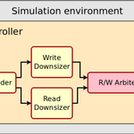
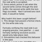
Today's bug of the week is a story. It starts with a commercial memory controller (built by yours truly), that passes all of its simulation tests. Reads tested, writes tested, WRAP tested, Exclusive access checked, etc.
Many, but not all components were formally verified.

Formally verifying the components involved required building proper interface property sets--to make sure any input assumptions were guaranteed by the prior component and so on. In the process, another bug was found whereby reads (or writes) crossing different devices might get merged. Likewise, reads might have accidentally merged requests across WRAP requests--turning WRAP requests of the H/W into hybrid WRAP requests--even though not all memories support hybrid wrap.

One subtle reality, is that the two streams (read/write) of such a cache cannot be independent. If nothing else, they will need arbitration to access tag memory. This is in contrast to most of my AXI work, where I try to keep the read/write FSMs as independent as possible.
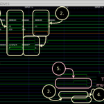
This stack exchange post has a good description of the problems with using AES-CTR for memory encryption. I love the included pictures. They tell the story well.
crypto.stackexchange.com/que…
One of the differences between ASIC and FPGA design is the initial statement. ASICs don't support them. To build IP that works across technologies, I've had to be very careful where, when, and how I use such statements. In many cases, I've had to remove them over time when my FPGA designs later become ASIC designs.

Arguably, the impact of any initial statements within a design on tainting any simulation results is a very real and valid threat to verifying any would-be ASIC IP, so I get their point.
Some time ago, I posted an article on how to move values and strobes across clock domains. The module was powerful, very versatile, and easy to work with.
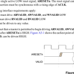
It had one flaw: it required a reset that would active in both clock domains at the same time, then synchronously release.
I love the technique. I use it often. It's become a go-to approach for moving everything across clock domains slowly. As a result, the logic quietly moves from one project to another. It's now been in a couple ASIC projects as well.
Here's the post for reference:
zipcpu.com/blog/2020/10/03/t…
Here's the kicker. In one ASIC project, I was trying to cross from the JTAG clock domain to the system clock and back again. The two domains had separate and independent resets. To be useful, I had to AND the two negative edge resets together, then synchronize their release to get the CDC module to meet its formal assumptions.
Crossing reset domains like that breaks timing. I could no longer guarantee setup and hold timing on any of two individual reset paths, I could only accept the violation, accept that it would yield uncertain results for a clock cycle or two, and then go on. It's not ideal, and the hand-waiving stinks.
If you can think of a better solution, let me know and I'll try it.